
Explore Millennium Ecosystem

India's First Silicon Moment — And the Gap Nobody Has Filled Yet

Laxmi Khengare
AI innovation
- 26 June 2026
- 10 min read
India's First Silicon Moment — And the Gap Nobody Has Filled Yet
Laxmi Khengare
AI innovation
- 26 June 2026
- 10 min read
Key Takeways
- India’s Semiconductor Ecosystem is growing rapidly, but limited access to First Silicon Bring-Up and Post-Silicon Validation infrastructure continues to slow the journey from chip design to commercialization.
- First Silicon Bring-Up is one of the most critical stages in semiconductor product development, where engineering teams validate functionality, characterize performance, and identify potential design or manufacturing issues.
- Semiconductor Testing and Validation capabilities are becoming strategic enablers for Fabless Startups, helping reduce development risk, improve product reliability, and accelerate time-to-market.
- AI-Powered Validation and Automated Failure Analysis can significantly shorten debug cycles by enabling faster root-cause identification, intelligent test optimization, and data-driven engineering decisions.
- A stronger collaboration between Design Houses, Semiconductor Startups, Testing Labs, Foundries, and Technology Providers is essential to building a resilient and globally competitive semiconductor ecosystem in India.
- Organizations that bridge the gap between Silicon Innovation and Product Commercialization will play a pivotal role in supporting India’s ambition to become a global semiconductor powerhouse.
- The future of India’s Semiconductor Industry depends not only on designing more chips, but also on validating, qualifying, and scaling those innovations efficiently for global markets.
Introduction
India is rapidly emerging as a global semiconductor powerhouse. The country contributes a significant share of the world’s chip design talent, government initiatives are accelerating ecosystem growth, and a new generation of fabless startups is pushing the boundaries of innovation.
Yet for many semiconductor companies, the real challenge begins after the chip has been designed.
The transition from tape-out to first silicon validation remains one of the most critical—and often overlooked—stages in the product development lifecycle. It is the moment when engineering assumptions meet physical reality, when months of design effort are put to the test, and when startup timelines, budgets, and commercialization plans can be significantly impacted.
While India has made remarkable progress in semiconductor design capabilities, gaps in post-silicon validation, testing infrastructure, and bring-up support continue to create hurdles for emerging innovators.
This article explores why first silicon bring-up has become a strategic bottleneck for India’s semiconductor ecosystem, the opportunities it creates for ecosystem players, and how advanced testing and AI-powered validation can help bridge the gap between silicon innovation and commercial success.
When a Billion-Dollar Blueprint Meets a Small Box of Sand
India is having its semiconductor moment. The headlines are loud, celebratory, and impossible to ignore—mega-fabs, Advanced Trench Merged Pin (ATMP) units, government incentives, and high-profile MoUs signed at Semicon India. Tata Electronics is breaking ground; Micron is rapidly expanding its footprint in Gujarat. Policymakers talk about custom silicon with the same historic optimism once reserved for the software boom. It feels like a national transformation, and it genuinely is.
But working inside Millennium Semiconductor—at the intersection of high-precision chip testing and AI-powered certification—I spend my days looking past the press releases. I look at the physical realities of the factory floor and the engineering lab. When you strip away the macroeconomic commentary, there is a gaping vulnerability in India’s semiconductor roadmap that almost nobody is talking about.
It is the perilous journey a chip takes the exact moment it leaves the software simulation and enters the real world.
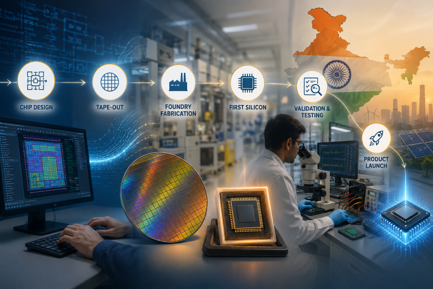
India’s emerging semiconductor landscape: Moving from design code to physical silicon testing
The Paradox at the Heart of India's Chip Story
To understand why this gap matters, one must look at the structural irony defining India’s tech ecosystem. Every year, domestic engineers design approximately 30,000 chips. Our talent pool populates the core engineering teams of global semiconductor giants—Intel, Qualcomm, Texas Instruments, NXP, Infineon, and AMD. In fact, India represents roughly 20% of the world’s semiconductor design workforce.
And yet, India’s domestic fabless chip industry generates less than $50 million in annual revenue. The structural talent has always been here, but the Intellectual Property (IP) goes abroad. Indian engineers design the world’s chips, but global corporations own the equity and profit. That is the paradox India’s semiconductor policy is now aggressively trying to break.
The India Semiconductor Mission (ISM), the Design Linked Incentive (DLI) scheme, and the Chips-to-Startup (C2S) program are all coordinated attempts to encourage Indian engineers to stop building other people’s chips and start building their own. For the first time in our industrial history, it is working.
A new generation of Indian-founded, VC-backed fabless chip startups is emerging. Companies like Netrasemi (AI vision SoC), Morphing Machines (reconfigurable processors), Calligo (RISC-V HPC co-processors), and BigEndian are led by industry veterans with 10 to 20 years of experience shipping production silicon at companies like Intel and Qualcomm. These are not academic experiments or college projects. These are world-class hardware teams building complex, serious commercial silicon.
INDUSTRY SNAPSHOT: THE PUNE-BANGALORE SILICON CORRIDOR
- Projected Market Scale: India is projected to cross $100 billion in semiconductor market value by 2030.
- VC Pivot: In 2025, 22% of Indian Venture Capitalists identified semiconductors as their absolute top investment priority.
- Design Dominance: India anchors approximately 20% of the world’s semiconductor design workforce, yielding over 30,000 chip designs annually.
- The Revenue Void: Domestic fabless revenue remains a modest gap at under $50 million annually, highlighting the need for commercial IP retention.
The Unforgiving Lifecycle of 'First Silicon'
Here is where I want to slow down, because this is the operational choke point that mainstream semiconductor commentary skips entirely. When a fabless startup finishes designing a chip, they send the software blueprints (GDSII files) to a foundry like TSMC, GlobalFoundries, or eventually the new domestic fabs coming online in Gujarat and Assam.
The foundry fabricates the chip on silicon wafers, packages them, and months later, the startup receives a small, unremarkable box. Inside that box is what the industry calls ‘first silicon’—the very first physical instance of a chip that previously existed only as code on an engineer’s monitor.
It is one of the most thrilling, terrifying, and significant milestones in a hardware company’s lifecycle. First silicon may work perfectly, partially work, or fail to boot entirely. The startup does not know why, and they have roughly six months of financial runway to find out.

First silicon bring-up is the ultimate stress test for a hardware startup. It is where pure software logic collides with physical anomalies, ambient noise, and thermal realities. It is not a vendor interaction; it is a battle for company survival.”
Where Do Indian Hardware Startups Go Today?
- ChipIN / SmartSoC (via C-DAC): While providing critical post-silicon validation services, this government-backed infrastructure is restricted strictly to startups registered under the state’s DLI scheme. This covers a small, highly subsidized subset of the market. Capital-backed startups that do not qualify for or require DLI sit entirely outside this umbrella.
- Tessolve Semiconductor (Bangalore): A highly competent commercial laboratory with robust, 24/7 post-silicon validation capabilities. However, their commercial model is built around enterprise clients with high-volume production guarantees. They are not structurally aligned to support an early-stage startup that has received 50 engineering dies and requires intense, fluid, exploratory bring-up support.
- Tier-1 Global OSATs: Global giants like Amkor or ASE provide exceptional engineering services, but their minimum order quantities (MOQs) and turnaround queues are engineered for massive production pipelines, not agile, rapid-turnaround prototype characterization.
The operational result is highly predictable. Indian hardware founders are forced to pack up their test boards and fly their engineers to Hsinchu, Taiwan, or Silicon Valley. They pay steep international consulting rates and lose precious weeks to travel and customs logistics. Alternatively, they grind through bring-up internally using makeshift labs and a handful of engineers who may have never managed a physical bring-up cycle from scratch.
Nobody in India is currently positioned to tell an early-stage founder: ‘Bring your first silicon to us the afternoon it arrives, and we will walk through the bring-up trenches with you side-by-side.
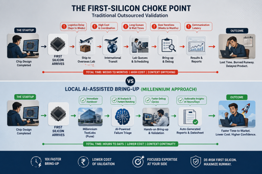
The First-Silicon Choke Point: Comparison between traditional outsourced validation and local AI-assisted bring-up
The Ecosystem Bridge India Still Needs
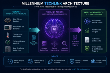
This is the precise gap Millennium Semiconductor is uniquely positioned to fill. Our organization operates two distinct, powerful business divisions: Millennium Test Labs, which provides advanced physical semiconductor testing infrastructure, and Millennium TechLink, which is engineering an advanced AI-powered automation and certification platform. When you map these combined capabilities against the first-silicon bottleneck, the commercial and technical fit is striking.
Our Test Labs division already possesses the physical instrumentation needed for rigorous chip characterization—parametric testing arrays, automated temperature/voltage sweep chambers, and the precise debug methodologies that first-silicon bring-up demands. Concurrently, TechLink is building the underlying data platform and automation layer designed to ingest raw, unformatted parametric test data and instantly output highly structured, standards-compliant certification reports and technical datasheets.
The strategic leap involves synthesizing these layers. Millennium’s vast repository of historical test data—spanning years of pass/fail results, physical failure signatures, and resolution pathways—can serve as the foundational training set for a specialized Industrial AI layer focused exclusively on accelerating post-silicon debugging.
One of the most significant discoveries was the variability of the acoustic environment. Noise conditions changed throughout the day and differed across stations. Static noise models were insufficient, requiring adaptive noise estimation.
- High-Touch Bring-Up Support: Immediate physical lab access to verify baseline power-on sequences, map thermal gradients, identify non-responsive blocks, and establish a clear parametric baseline.
- AI-Assisted Failure Triage: When a specific block on the ASIC behaves anomalously, our domain-tuned AI layer searches historical failure signatures to retrieve the closest analogous bugs and their specific physical resolutions. A mid-level validation engineer can form a robust diagnostic hypothesis in hours rather than weeks of isolated guesswork.
- Automated Datasheet & Compliance Generation: Techlink’s automated software ingestion layer takes the characterization data directly from the test benches and auto-generates a clean, standard-formatted technical datasheet. This is the exact artifact a startup needs to prove to investors, prospective enterprise customers, and global supply chain partners that their silicon is real, validated, and repeatable
The most valuable asset in the semiconductor race is not just fabrication capacity—it is the speed at which a design graduates from a physical prototype into verified, market-ready IP.
Why the Window of Opportunity is Open Right Now
Timing is everything in electronics hardware. The first wave of well-funded Indian fabless startups that taped out designs over the past twenty-four months are expecting their physical first silicon to arrive back from international foundries between late 2025 and 2027. This is our specific commercial window.
Once this window closes, long-term engineering relationships will crystallize. Every hardware startup that successfully navigates its first grueling chip bring-up will permanently remember the laboratory and the engineering team that stood by them in the trenches. That is not a transaction-based vendor relationship—it is an embedded, foundational partnership. The enterprise that earns that institutional trust over the next twenty-four months will remain deeply woven into the fabric of the Indian semiconductor ecosystem for the next decade. Every month we delay positioning our capabilities is a month of that irreplaceable window closing.
The Validation Roadmap: Three Strategic Conversations
To validate this corporate positioning immediately, we must answer three clean operational questions through targeted action:
- Data Asset Audit: Does our TestLabs division possess a sufficiently clean, structured archive of historical validation data to train an initial AI failure triage prototype? If yes, our highest-barrier proprietary asset already exists.
- Platform Capability Check: Can Techlink’s current automation software ingest tabular parametric data and output an industry-standard technical datasheet without manual developer intervention? If largely yes, our documentation layer is structurally complete.
- Direct Founder Engagement: We must directly contact the leadership teams at Netrasemi, Morphing Machines, and BigEndian to conduct qualitative interviews on how they managed their first silicon bring-up. If they confirm that they struggled internally or spent heavily to export the work to overseas labs, our market demand is definitively validated.
Conclusion
Frequently Asked Questions (FAQs)
1. What does it mean to position a company as an innovation ecosystem bridge?
2. Why is ecosystem collaboration becoming critical in Industry 4.0?
3. How can AI help organizations strengthen engineering and innovation ecosystems?
4. What are the benefits of an integrated engineering and testing ecosystem?
5. How are companies preparing for the future of connected innovation?

About the author:
Laxmi Khengare
AI-innovation
Laxmi Khengare is a member of the AI Innovation team at Millennium TechLink, where she focuses on exploring emerging technologies and their real-world applications across industries. Her work spans AI-driven solutions, digital transformation, and innovation-led problem-solving, with a keen interest in how advanced technologies can accelerate business growth, operational efficiency, and technological advancement.
table of contents
- Introduction
- When a Billion-Dollar Blueprint Meets a Small Box of Sand
- The Paradox at the Heart of India's Chip Story
- Industry Snapshot – The Pune-Bangalore Silicon corridor
- The Unforgiving Lifecycle of 'First Silicon'
- Where Do Indian Hardware Startups Go Today?
- The Ecosystem Bridge India Still Needs
- Why the Window of Opportunity is Open Right Now
- The Validation Roadmap: Three Strategic Conversations
- Strategic & Industrial References
- Frequently Asked Questions (FAQs)